לוגו
  • Home
    • History
  • People
    • Faculty
    • Staff
      • Management
      • Administration
      • Clean room
      • Facility
      • Lab Engineers
    • Advisory Committee
      • Local Advisory Commitee
      • International Advisory Committee
  • Safety
  • Equipment
    • Photolithography
    • Nanopatterning
    • Etching
    • Deposition and Annealing
    • Characterization and Analysis
    • Packaging
    • 2D Center
  • Education
    • Academic Courses
    • Training Courses
  • Publications
  • Research
  • Working with us
  • Collaboration
    • Industrial Collaboration
    • Academic Collaboration
  • Events
    • All Events
    • Seminars
    • Conferences
  • 3D Facility Tour

Research

Description.

  • Encapsulated Franklin Oscillator Capable of 200,000,000 Switching Cycles

  • A Combustion Type Gas Sensor Based on Micro Machined CMOS Transistor with Pt Nano-Particles Printed Catalytic Layer

  • A new method to fabricate ultra thin transmission lines

  • Demonstration and Physical Analysis of Oxide Field Effect Transistors

  • Reconfigurable Radiofrequency Circuits based on Phase-Change Materials

  • MNFPU Equipment

  • Access doping of 2D MoS2 monolayers: Early fabrication process steps

  • Integrating nanofluidics with nanopores

  • Research & Development Highlights 2019

  • Effects of titanium layer oxygen scavenging on the high-k InGaAs Interface

  • Three port Josephson junction embedded in a superconducting DC-SQUID

  • Light Direction-dependent plasmonic enhanced GaNAIN quantum cascade detector

  • Transport Phenomena2

  • Transport Phenomena

  • Sensitive Magnetic Resonance Signal detection

  • Resopnsivity Enhancement of MIS Photodetectors by Plasmonic Nano Antennas

  • Quasicrystal Metasurface

  • Presence sensor

  • Photonic spin controlled multifunctional shared aperture antenna array

  • Indium Phosphide Nano Flags

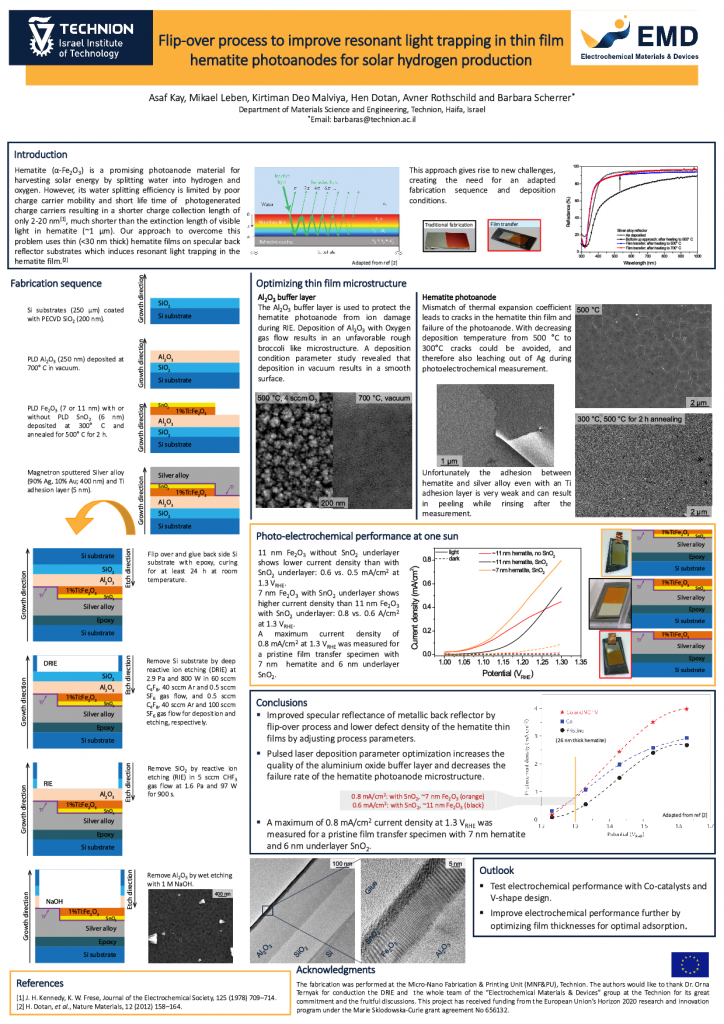
  • Flip-over process to improve resonant light trapping in thin film hematite photoanodes for solar hydrogen production

  • Fabricating Vertical Organic FET’s Patterned and coating the source electrode

  • Bio-inspired Growth of single crystal Nanoporous Gold

  • 1D and 2D Numerical simulation of electrical currents in excitonic solar cell

  • Avi Shriki Project

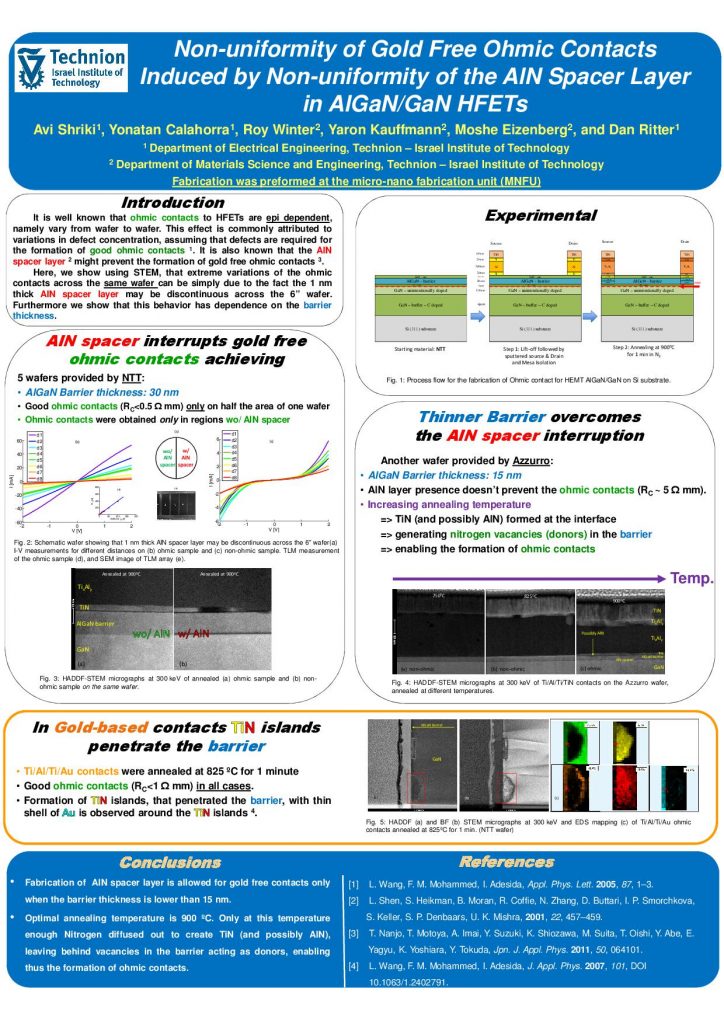
    Non-uniformity of Gold Free Ohmic Contacts Induced by Non-uniformity of the AlN Spacer Layer in AlGaN/GaN HFETs

  • Accessibility Statement

Useful Linkes

  • Home                    
  • Nanorob               
  • Technion Research Infrastructure
| Powered byFatfish